High Level Design
“HOW is your project build.” - Architecture: Partitioning and Interfaces
Hardware top level block diagram
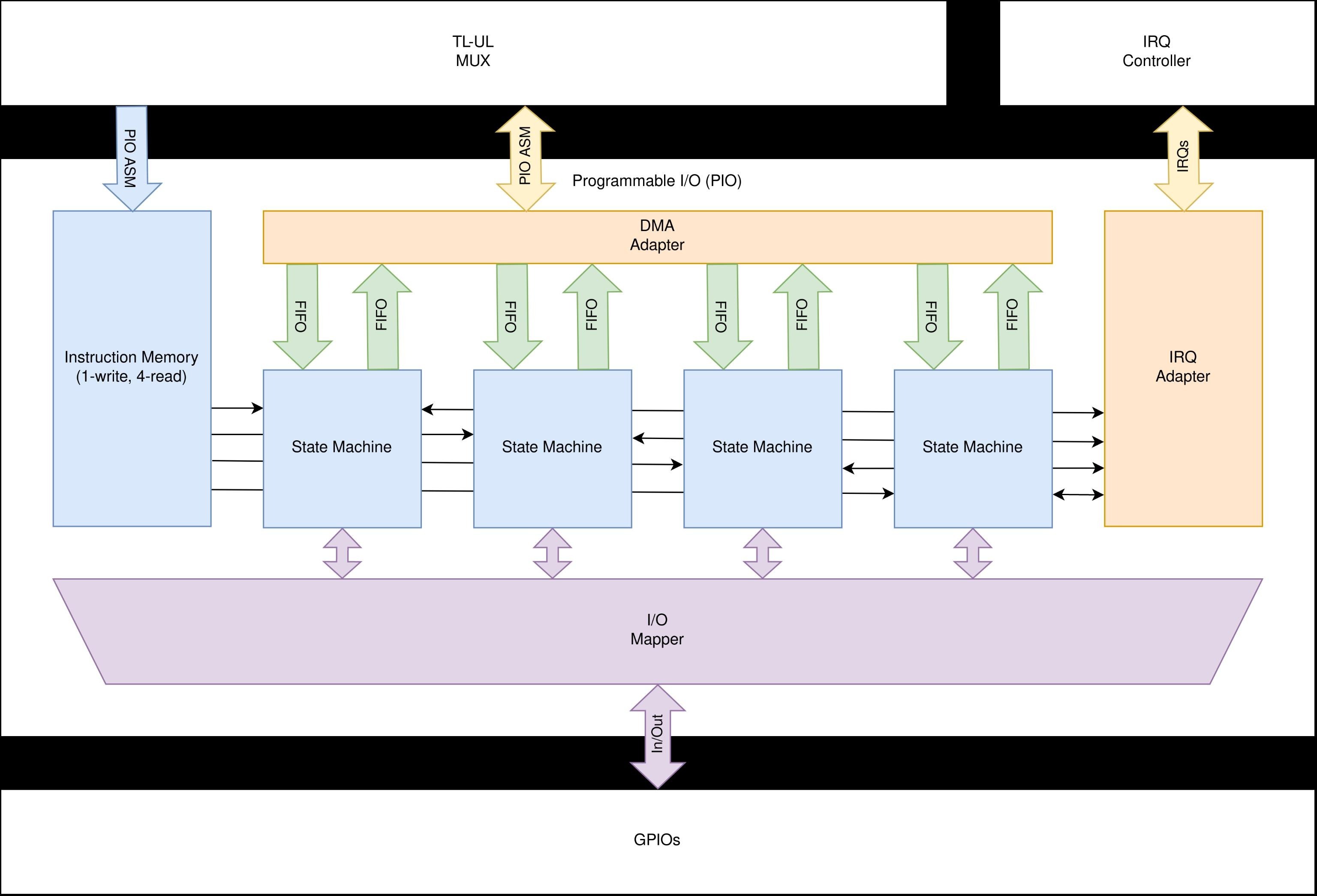
Contains at least
operating environment (e.g. hardware connected to the FPGA)
all connections to the environment using descriptive signal names
all HDL modules
all connections between the HDL modules using descriptive signal names
Focus should be the student level and your modules, the rest of the (supplied) rvlab shall be drawn in an abstracted manner.
This picture is the most important part of your entire documentation!
Software top level block diagram

Contains at least
all SW modules (HALs, libraries, major application components)
all relationships between SW modules. Exception: Shared libraries can be displayed separately.
show which SW module(s) access which HW module
Module specification
Functionality, interface and verification of each module.
If a functionality is identical to the Functional Specification do not copy, just refer.
Verilog module PIO
Function:
Top level module of programmable IO block
Interface:
student
TL-UL
rvlab_core
bram_main
GPIOs
Verification plan:
Run the for examples mentioned in the Requirements & Functional Specification
Additional notes:
Verilog module Instruction memory
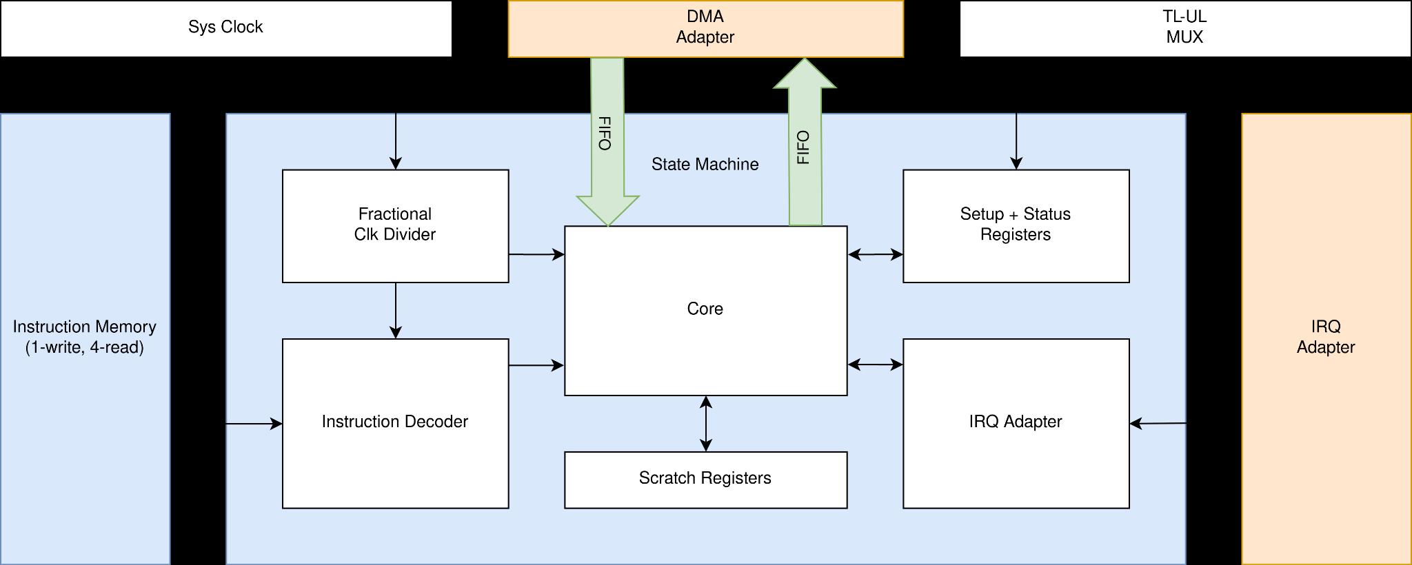
Verilog module State machine
Verilog module Fractional divider
Verilog module Instruction decoder
Verilog module Core
Verilog module Program counter?
Verilog module Scratch registers
Verilog module Setup + Status registers
Verilog module Output shift register (OSR)
Verilog module Input shift register (ISR)
Verilog module FIFO
Verilog module DMA Adapter
Verilog module IRQ Adapter
Verilog module IO Mapper
Verilog module X
Mandatory for each verilog module
functionality: brief, in bullet point form. Should be identical to the header comment of the verilog module.
interface
generated HTML of the register definitions (if the module has CPU accessible registers)
DMA descriptors (for TL-UL hosts)
block memory layout (if used, e.g. video memory)
verification plan: bullet points of the tests to be performed by your C code
Add everything else a programmer needs to know to use your module (e.g. timing diagrams, pseudo code for complex algorithms executed in HW, …)
HW module Y
Extension PCB / hardware build for this project.
functionality: schematic
interface: label all connections on the PCB as in the schematic to allow reuse in future projects.
PCB checklist
power supply
case a: only use the IO supply provided on the PMOD / FMC connectors
case b: use of any external supply or any DCDC converter requires galvanic isolation of all signals (e.g. using ADUM) (due to power sequencing requirement of the FPGA, sensitivity to any other voltage than the IO voltage)
schematic review of tutor
direction / pin mapping check before connecting to FPGA
extension PCB: power up separately (i.e. not connected to FPGA).
output pin check: Measure voltage at every output pin.
input pin check; Connect every input pin via a 10k resistor to VDD and VSS and measure the voltage (should be VDD and VSS, respectively)
FPGA
output pin check: Measure voltage at every output pin.
input pin check; Connect every input pin via a 10k resistor to VDD and VSS from the PMOD and measure the voltage (should be VDD and VSS, respectively)
SW module Z
“SW module” refers to a major SW components such as your application. HALs do not need to be documented.
Mandatory for each SW module
functionality: brief, in bullet point form. Should be identical to the header comment of the C file.
interface: function signatures and data structures
Optional
verification plan: Saves more time than it costs. Anyway, optional.